PSV3 Soldering Iron Hack - Part 2
reverse engineering soldering iron stm32This is the sequel to PSV3 Soldering Iron Hack - Part 1 where I already introduced the result of this whole project: a quite usable replacement firmware. Now let's see how we got there (so I guess it's rather a prequel).
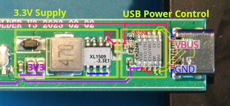
I already showed my annotated board layout:
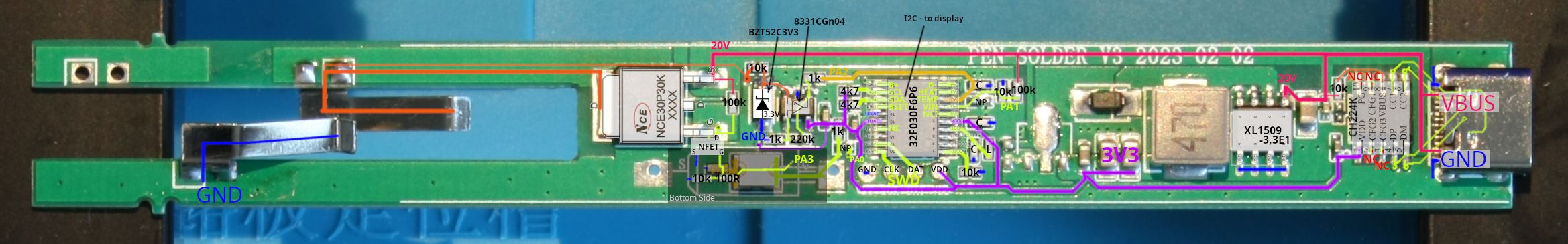
It was really helpful to create this image to get a first level of understanding about what's going on in this soldering iron. I made photos of the top and the bottom of the PCB,[1] added them as semi-transparent image layers in GIMP and traced the signals and parts in additional layers by hand/mouse.
Based on that image I created a reverse engineered schematic (PDF) in KiCad, which has also been a handy reference while developing the new firmware. For purposes of documentation though in this post I believe a kind of top-down block diagram is a better starting point.
Soldering Tip #
Let's start with a view of the parts around the soldering tip:
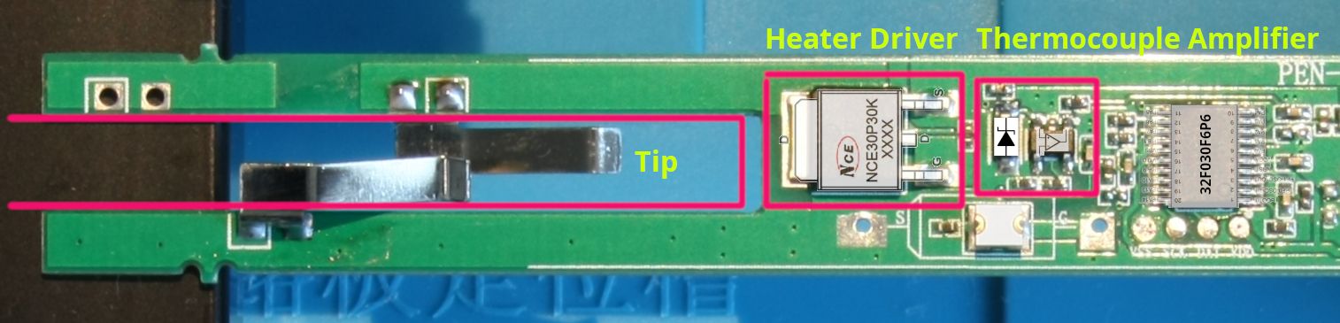
On the left you can see two contacts for the T12 soldering tip and connecting to those, the 20 V high-side heater driver MOSFET, and the operational amplifier for the tip's thermocouple temperature measurement.
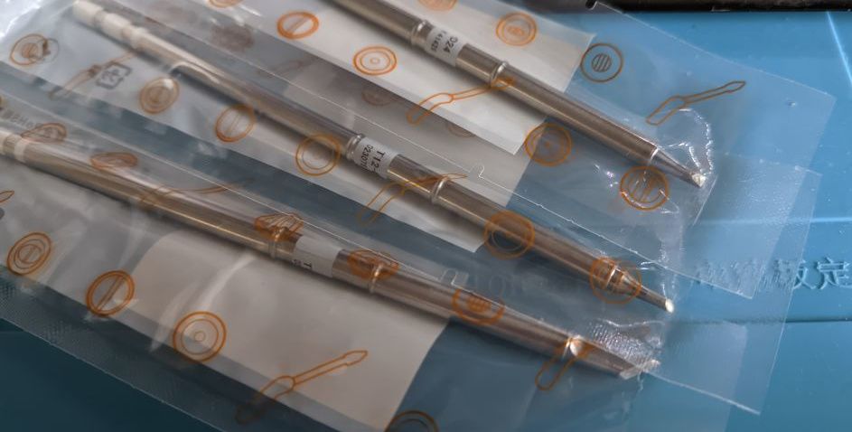
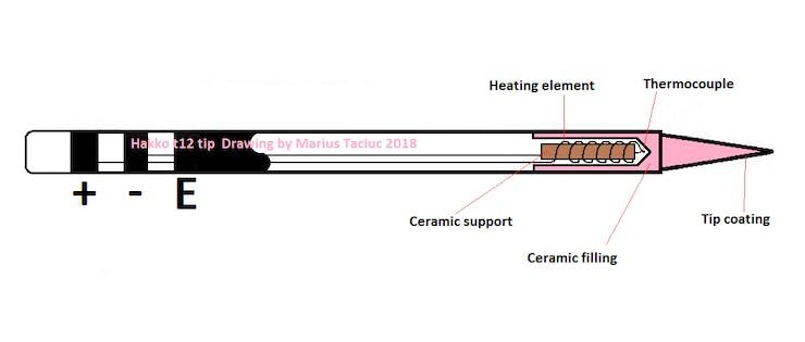
Hakko T12 compatible soldering tips are used by many cheap soldering irons and soldering stations (and by a few good ones). It's an active soldering tip so the heat is generated close to the tip leading to fast heat up times. Temperature measurement is also already integrated using a thermocouple. Both are connected in series between two pins (here marked -/+ while E is for Earth and not connected in this low voltage soldering iron):
Heating #
To heat the soldering tip we just apply our supply voltage to the pins (-/+ in the image above, TIP_A/B in the schematic below). This happens to always be 20 V in our case.
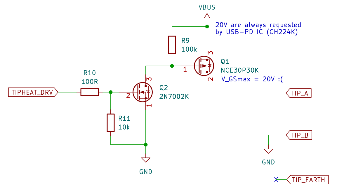
On the left we have a pin of the microcontroller (signal TIPHEAT_DRV) controlling a simple driver stage with a small N-MOSFET (Q2 here, its marking is 72K) which controls a P-MOSFET (Q1 here) that switches 20 V (VBUS) going to the tip on or off.[2]
During the heating phase we can model the soldering tip as a simple resistor. With a multimeter I measured its resistance to be ~8 Ohm (on my T12-B2 tip). So we can expect a theoretical maximum output of 50 W given the fixed supply voltage.
To regulate the heating element to get a stable temperature level we're switching the tip power with PWM to achieve a finer grained average output power. The desired output power is calculated by a PID controller (adapted from IronOS) that runs at 10 Hz which coincidentally is the same as the PWM frequency we're using.[3]
Temperature measurement #
Inside the tip there's a thermocouple connected in series with the heating element and thanks to the Seebeck effect, we can measure a voltage between the - and + pins which is related to the tip's temperature. But this works only when the heating element is turned off — otherwise you would just measure the 20 V that the power MOSFET connects to those pins.
Therefore we need to turn the heat off regularly for a fixed minimal amount of time; we need to wait for the temperature to stabilize a bit before taking ADC voltage samples. IronOS implements a bit more finesse at this point by filtering the measurements but it seems to work well enough to just increase the ADC sample time by a bit (like the stock firmware does, too).
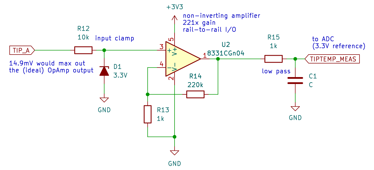
With only e.g. ~11.3 mV at 450 °C the voltage of the thermocouple in our operating range is too small to measure directly with the ADC of our microcontroller. That's why we have a non-inverting amplifier op amp circuit to boost this voltage (e.g. to ~2.5 V at 450 °C).
Temperature conversion #
Funnily enough there is a bit of a disagreement whether the type of the thermocouple in T12 tips is Type K, C, N, or whatever. I can't say which one is correct but either way it is going to be a linear temperature relationship between voltage and temperature in our operating range. So I made a round of rough measurements to get some input data for the PID controller.
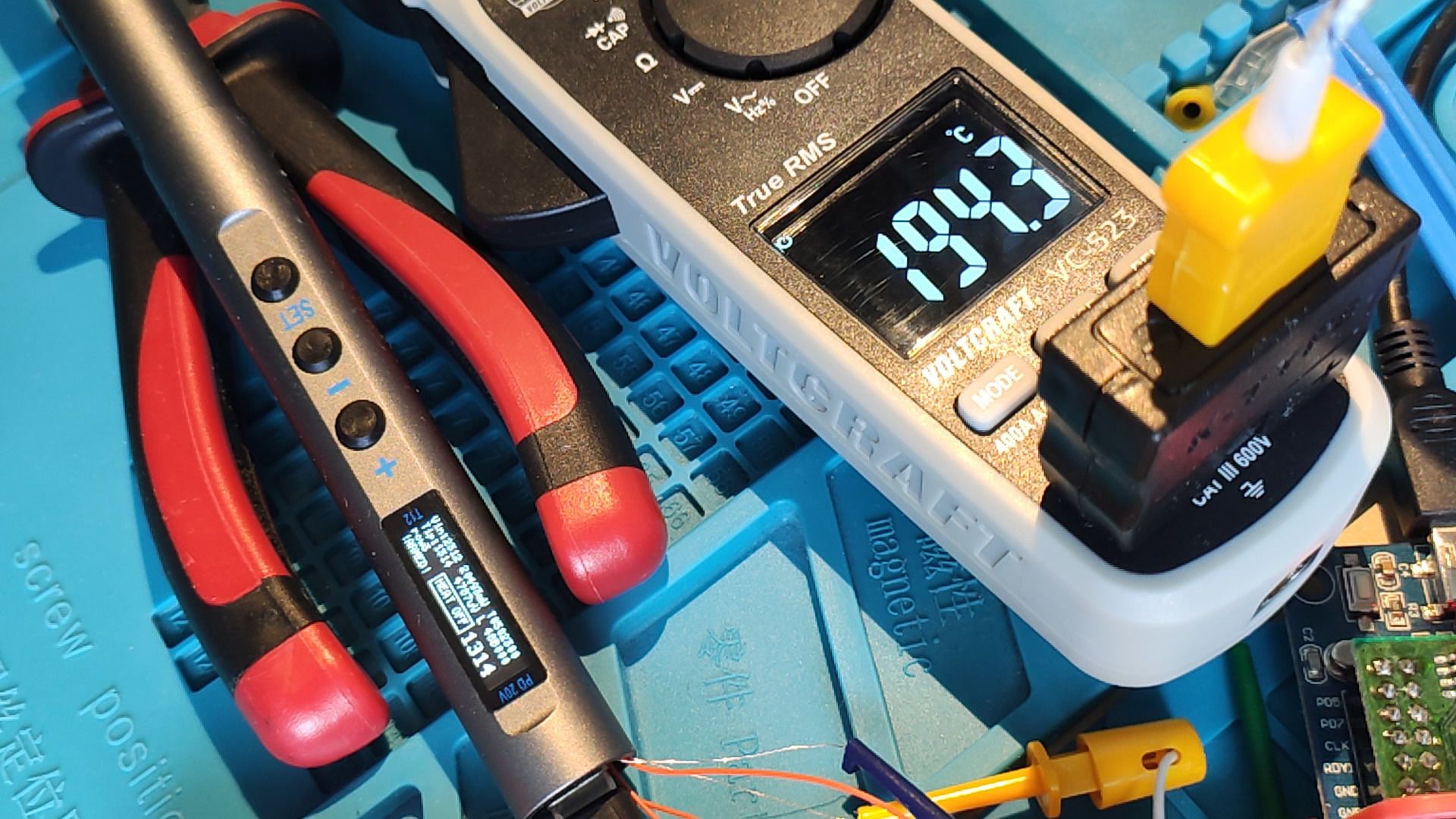
I used the temperature mode of a Voltcraft VC-523 multimeter, held it to the soldering tip, printed the raw ADC values in big numbers on the OLED display and filmed a video showing both the multimeter's and the iron's displays. Then I noted a bunch of temperature/ADC value pairs and did a linear regression in GNU Octave (soldering_tip_linear_reg.m, raw data), which leads to the following graph with values converted to microvolts:
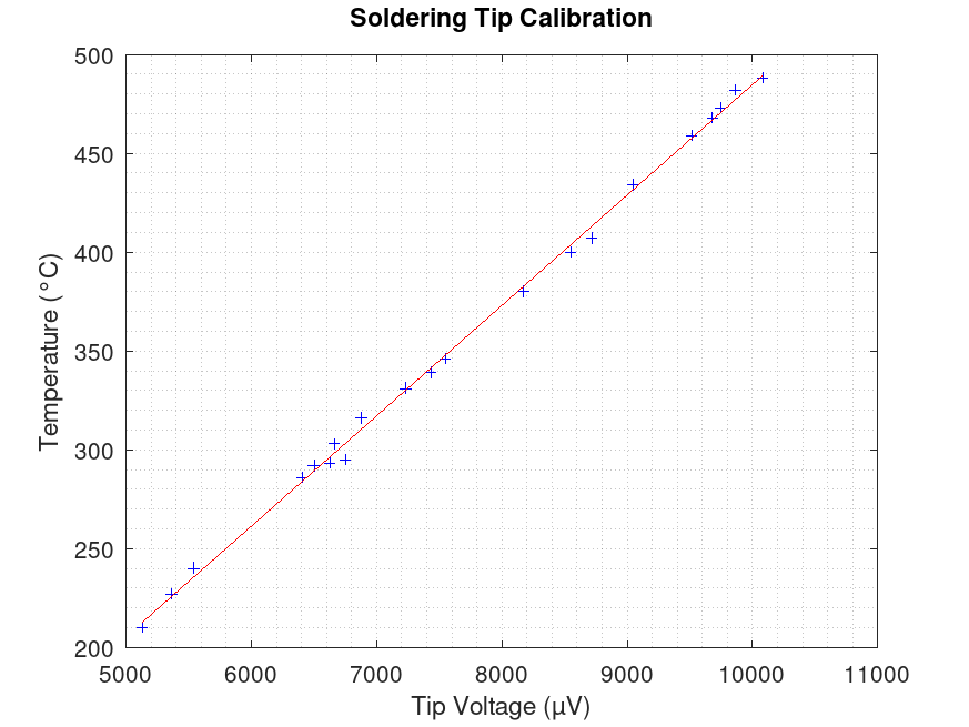
To implement my conversion function in the firmware I skipped the intermediate step and used ADC values directly to get the temperature in degrees Celsius with: T/°C = 0.2037 * x/(ADC units) - 73.8
This worked for a start and using this I was able to get pretty consistent temperature control, i.e. I set the soldering iron to hold 320 °C and the multimeter agreed within a few degrees with that.
But there are a few problems to consider with my calibration:
- Specialized devices to calibrate soldering iron temperatures exist (e.g. search on Aliexpress for "soldering iron calibration") — I don't know how using my multimeter's thermocouple compares to those.
- It matters where on the tip you measure. I tried to hold the sensor in a consistent position on the side of the tip where the solder would be but results in a different place will not be the same. (Maybe putting it in oil would be better?)
- I didn't consider cold junction compensation. So I probably have at least a fixed offset in my temperature control depending on the room temperature, thus I should probably subtract room temperature from the values. But then again this soldering iron doesn't have a separate sensor to measure ambient (or handle) temperature. Maybe this could be a setting in the GUI, though.
Finally, comparing these results with IronOS' temperature curve of a T12-style tip they're pretty similar in the range I care about most (i.e. above 300 °C) except for a static offset, which may be due to my missing cold junction compensation or due to measuring errors on my side. On the low end (below 200 °C) there are bigger disagreements. In any case I would trust their measurements more than mine, so I'm going with their interpolation table instead of my regression function for now.
USB supply control #
On the right half of the board the CH224K Low-cost USB-PD Sink Controller (datasheet) runs the show and configures the USB power supply over the USB-C pins DM/DP/CC1/CC2. USB Bus Voltage VBUS then powers the soldering tip and it's also the input voltage for an XL1509 3.3 V buck regulator (datasheet) that powers everything else on the board.
USB-PD controller #
The CH224K gives two options to configure the voltage it requests from the USB power supply: A resistor connected to pin CFG1 or high/low logic levels setting pins CFG1/2/3, which would be quite interesting if they were connected to a microcontroller.
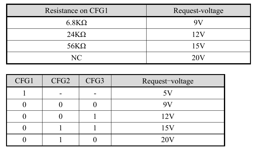
Sadly, on this board the CFGx pins are not connected to anything, so 20 V is always chosen for VUSB. I'm thinking about connecting a 56 kΩ resistor to CFG1 though to select 15 V and give the P-MOSFET a longer life.
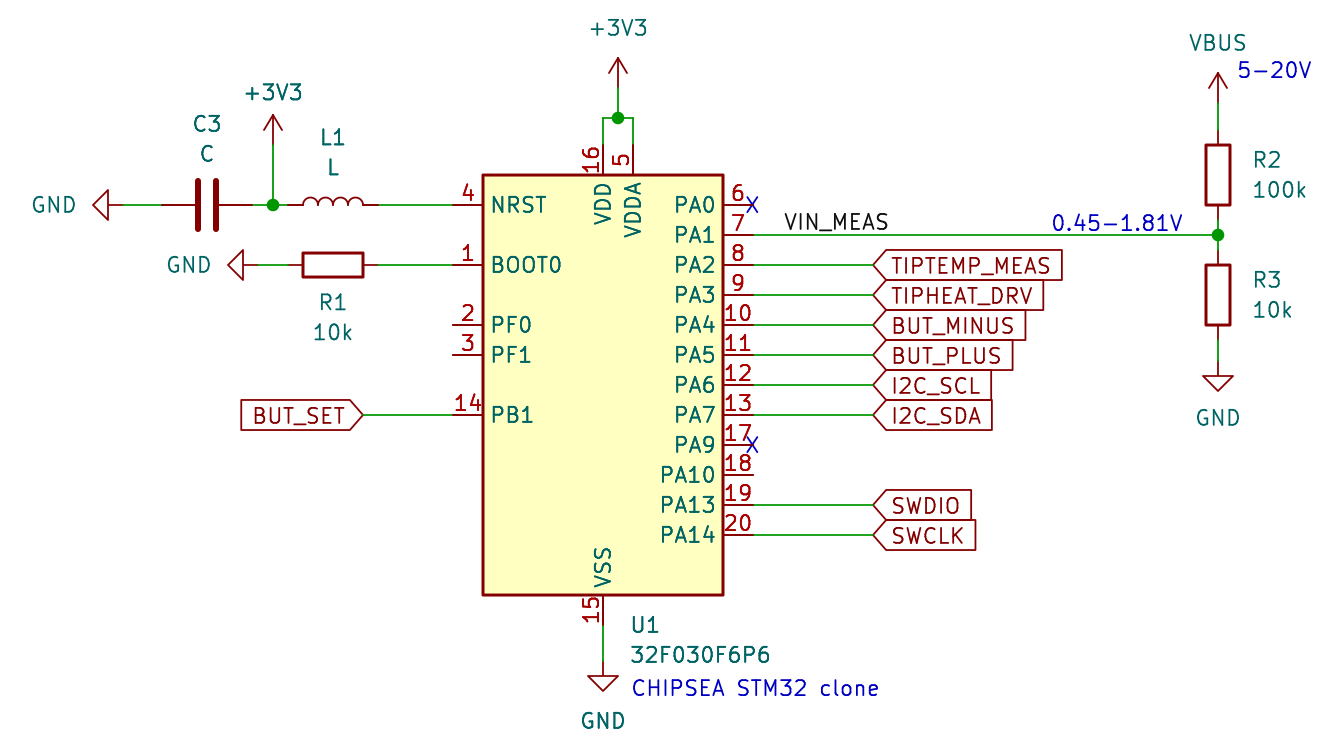
Microcontroller #
The microcontroller is an STM32 clone named CHIPSEA 32F030P6F6. It seems to behave pretty well and I didn't have any problems with the ADC or otherwise.
This design has some annoying quirks though:
- The OLED I2C display isn't connected to the also available hardware I2C pins but to random I/O pins, so we have to use bit-banging to control the display.
- The tip heat driver (TIPHEAT_DRV in my schematic) is connected to
PA3which doesn't have PWM — the only timer channel on this F030 line is TIM15_CH2 and this particular footprint doesn't have Timer 15. - There is no way to reset the "STM32", e.g. for SWD debugging and also no UART/etc. output, so we need to test by pin wiggling until the display works
OLED display #
To find out how to talk with the OLED display I hooked up a logic analyzer to its I2C bus. As we can quickly see from all the I2C writes to address 0x3c it probably uses a SSD1306-compatible protocol, so in the best case we only need to replicate the used initialization sequence and can then use the u8g2 display library to render our display content and do the rest of the communication.
Bad code #
I had already found the display initialization code in the dumped stock firmware (of course I could have also used the logic analyzer to dump it, but I didn't trust it due to the weird NACK behavior mentioned below):
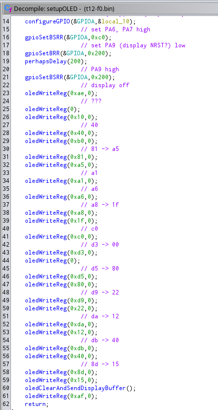
Funnily enough the stock firmware sends each of the bytes during the initialization in a separate I2C transmission (including start + stop condition, address byte, register byte) which takes needlessly long. You can just send the whole sequence in one transmission instead (and u8g2 does this btw.).
Another weird behaviour is that, going by the logic analyzer traces, the display doesn't seem to send ACKs — after every byte the bus master (i.e. the microcontroller) should let go of the SDA line and the slave should pull it low to indicate acknowledgement of that byte.
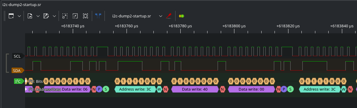
It turns out that the reason why the OLED display doesn't seem to send ACKs is because it can't — the stock firmware leaves the I2C SDA and SDL pins in push-pull mode the whole time. This means the high state on SDA is actively driven high by the microcontroller. When the OLED display tries to drive it low during the ACK/NACK period, we get some in-between voltage on the SDA line that can be seen with an oscilloscope (which my logic analyzer decoded as high).[4]
Also, as you can see in the initialization code above, they toggle PA9 before starting the display initialization sequence. While this pin is probably meant to be hooked up to the display reset line, it isn't connected to anything on this board.
Better code #
After some searching in the excellent u8g2 sources (and a lot of trial & error) I found the ssd1306 128x32 univision initialization which is pretty much the same as the one used on our soldering iron (plus display inversion/rotation settings which are done elsewhere in the stock firmware).
The bit-banging driver was quite slow though on an STM32. One reason is that it uses Arduino I/O functions like digitalWrite() which seem to be very slow in stm32duino (there are some pin and port lookups which probably take a few cycles each time). Once I switched to using the low-level I/O functions though I was able to get from ~26 kHz to ~89 kHz I2C clock speed.
With some further optimizations I finally got around 170 kHz. All together the whole display content is now rendered and transmitted in around 49 ms, which is well within the 100 ms PID controller and measurement period, so they don't interfere too much with each other (and due to the way I2C works, it shouldn't matter anyway if a clock cycle here or there is a bit longer).
Stock Firmware #
I already showed in the previous post how to dump the stock firmware using an STLink USB stick.[5] For analysis in Ghidra I found ghidra-stm32f0 quite useful — it's a loader that sets up memory regions and register names so you don't see reads and writes with addresses like 0x04001000 everywhere. (Be aware though that it labels many interrupt vector table entries that don't exist on our low-spec STM32F0 and are actually already code. Also it's missing a lot of timer and ADC peripherals that we're using but it's better than nothing.)
Initially I wanted to know how they're implementing their temperature controller but it wasn't that interesting anymore after the ported code from IronOS worked so well. There are always bits and pieces of display code or peripheral setup in between so the decompiled code is actually quite a slog to get through.
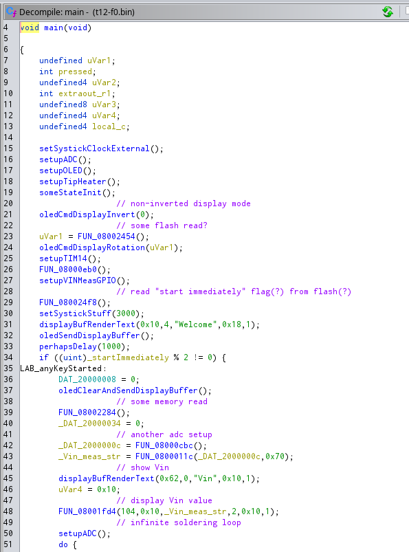
Custom Firmware #
For my custom firmware I started with a custom PlatformIO board that I derived from an existing one using another MCU of the F030 line. A board with this specific STM32F030F6P6 with 32 kB Flash and 4 kB RAM didn't exist so I had to create one. Peripheral initialization was a bit tricky because contrary to my expectations, stm32duino doesn't handle most of the clock setup of GPIOs/etc., so I ended up using STM32Cube to generate setup code for the system clocks and also the ADC and GPIO setup for me.
The core of my custom firmware is pretty simple: UI stuff (buttons + display) happens in the Arduino loop() function every 100 ms:

And soldering tip control is interrupt-driven by Timer 3 (TIM3), which resets every 100 ms (that interrupt turns the heat on) and is using 3 compare interrupts (1. heat off, 2. temperature measurement, 3. PID calculation):

The time at which the heat turns off is given by the desired duty cycle that the PID routine calculates. As discussed before, after turning off the heat we wait a fixed time for the temperature reading to stabilize (currently 10 ms, but this could be made shorter), and then take the ADC temperature reading.
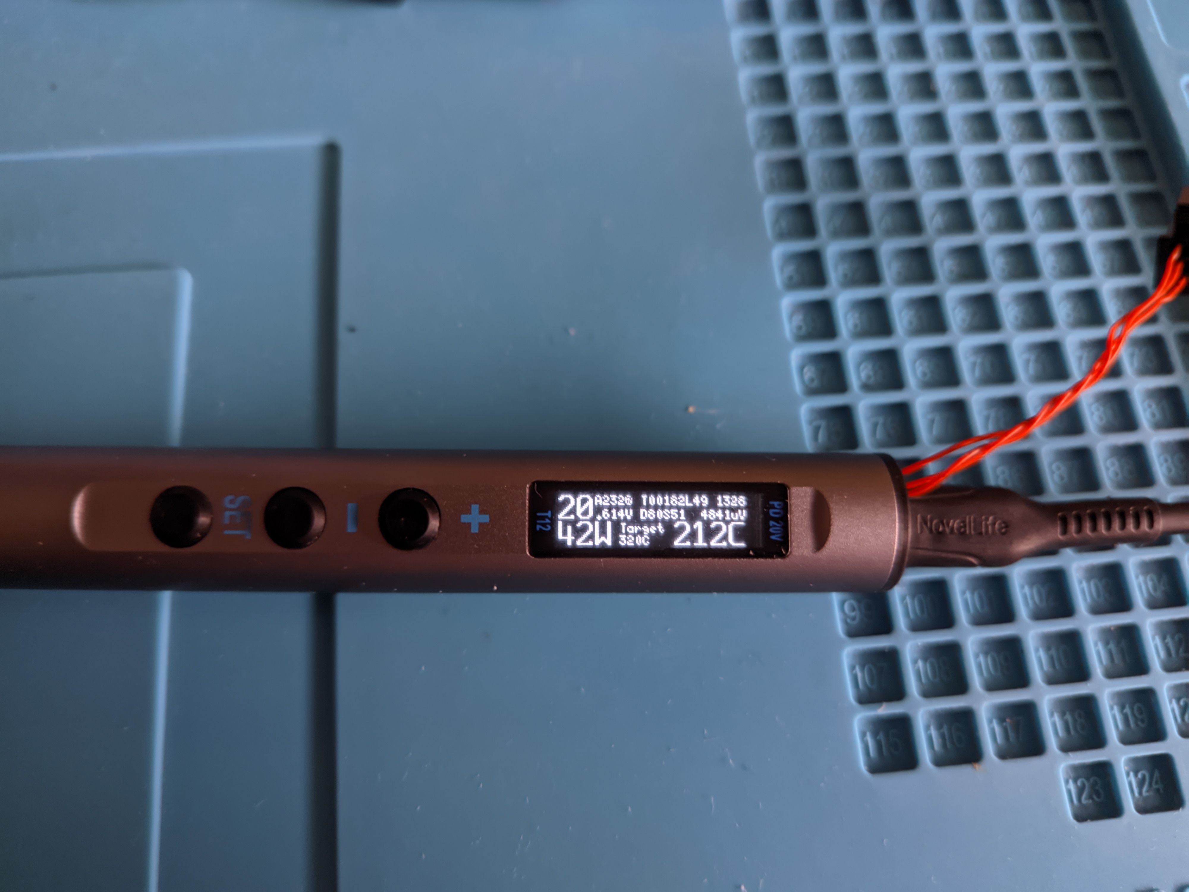
In the current state the GUI is pretty simple. It only consists of one screen, you can press SET to turn the soldering iron on or off, then it goes to stand-by after 60 s. And you can set the target temperature using the + and - buttons from 150 to 450 °C.
Of course, as already noted, I was able to take the PID controller code from IronOS with a few little changes and it gives really good results without even tweaking the parameters (using the ones from the Pinecil V2).
Results and further improvements #
I'm reasonably happy with the firmware at this point. It takes around 15 seconds to get from room temperature to 320 °C (and this, according to my limited measurement capabilities, really is 320 °C), while the stock firmware was way off with its temperature control, giving only around 280 °C when 320 °C are set. Temperature control during soldering is also rock solid.
Additionally, it might be a good idea to connect the USB-PD controller to a resistor to select a USB voltage of 15 V in order to improve the life-time of the P-MOSFET which is currently operating at its limit V_GSmax of 20 V. But this would come at the cost of longer heat-up times. Alternatively, you could replace that MOSFET with one of the few that withstand a V_GS of 25 or even 30 V.
Furthermore, cold junction compensation is currently being ignored and we can't probably do much without modifying the hardware. But we should at least be able to configure a fixed temperature calibration offset in the GUI like in IronOS.
Finally, it would be nice to get a soldering iron temperature calibration tool to make a more trustworthy calibration curve.
Links #
- Flashing Instructions (previous post)
- Firmware
- Schematic
Footnotes #
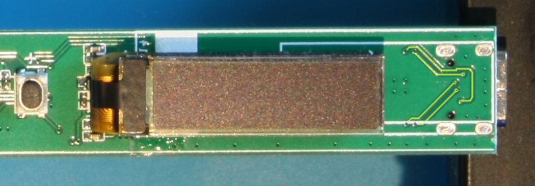
The bottom side of the PCB isn't very interesting so I'm skipping it here. You can look at it here. It pretty much only contains 3 buttons, the OLED display (we don't need to know more than that it's connected by I2C), and a small N-MOSFET driving the bigger P-MOSFET that switches the heat. ↩︎
The N-FET is needed because the microcontroller can't switch the gate of Q1 directly. ↩︎
IronOS implements another trick to get faster heat up times, but we don't (yet): They're using a lower 5 Hz PID rate and PWM frequency during the initial heating phase to get higher power output by allowing for a higher PWM duty cycle. The duty cycle can be higher because overhead of the time needed for temperature measurement to settle is constant (see next section). The trade-off for this higher output power is less accurate temperature control. ↩︎
The proper way to do handle this would be for the microcontroller to either configure the pin as open-drain (instead of push-pull) or to switch the pin from output to input. The latter one is also useful if you actually want to know what the slave responded. ↩︎
I haven't yet decided whether I want to publish that dump but if you're interested in (probably also shoddy?) soldering station firmware dumps, you can find some at https://github.com/deividAlfa/stm32_soldering_iron_controller/tree/master/Original_FW. ↩︎